
· Jiri Skapa, JSE · VORTARIAN · 6 min read
VORTARIAN 4R2T-10G Board Ports Description: RF, Clock, Trigger and Dual 10 GbE
A port-by-port guide to the VORTARIAN 4R2T-10G board: four coherent RF inputs, two RF outputs, a shared 100 MHz reference, trigger I/O and two 10 GbE links for low-latency communication, radar and SDR receivers.
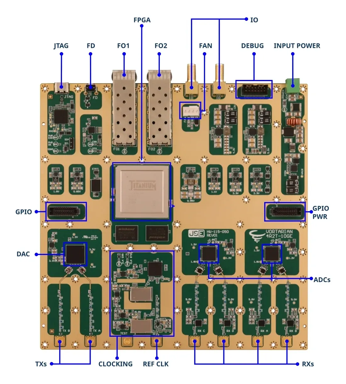
This article describes the ports of the VORTARIAN 4R2T-10G board: what each connector is, what it carries and how it is typically used in a radar or SDR receiver. The labels in the picture match the section headings below.
Overview
| Port | Connector | Function |
|---|---|---|
| RX A, RX B, RX C, RX D | SMA, 50 Ω | Four RF inputs |
| TX A, TX B | SMA, 50 Ω | Two RF outputs |
| REF CLK | SMA, 50 Ω | 100 MHz reference input or output |
| TEST | SMA | Clock test output |
| IO | 2× SMA | Trigger, PPS and synchronisation signals, 3.3 V |
| FO1, FO2 | SFP+ cage | 10 GbE data links |
| GPIO, GPIO PWR | High-density board-to-board | Digital I/O for user extensions |
| JTAG | USB-C | FPGA programming, JTAG and serial console |
| FD | Push button | Factory default |
| DEBUG | 2×7 boxed header | Service and debug access |
| FAN | 4-pin header | Cooling fan |
| INPUT POWER | Terminal block | 10 V to 14 V DC |
RF inputs: RX A to RX D
The four receive inputs are 50 Ω SMA connectors, AC-coupled. Each input has its own filtered and amplified RF path in front of one channel of a dual-channel ADC; RX A and RX B go to one ADC, RX C and RX D to the other.
- Direct sampling from 20 MHz to 1400 MHz; the standard build covers 250 MHz to 500 MHz.
- Maximum input level about −10 dBm. Higher levels can permanently damage the input.
- DC on the input must stay below 7 V; the inputs are ESD protected to ±20 kV.
All four channels are clocked from the same clock tree, so their sampling instants stay in a fixed relationship. This is what makes the board usable for phase-coherent work: passive and MIMO radar, direction finding and beamforming, where the phase difference between channels is the measurement.
RF outputs: TX A and TX B
The two transmit outputs are 50 Ω SMA connectors driven by a quad-channel DAC, with an output level of about −8 dBm. They share the clock tree with the receivers. In a radar setup they can generate the waveform or a calibration tone that is fed back into the receive channels to measure and correct their phase and gain.
Clocking: REF CLK and TEST
REF CLK is a 50 Ω AC-coupled SMA port that can be configured either as an input or as an output.
- As an input it accepts a 100 MHz reference, ±10 ppm, at +6 dBm ±3 dB (absolute maximum +9 dBm). A reference outside this range degrades phase noise.
- As an output it provides the board’s 100 MHz reference to other equipment.
With an external reference, several boards can run from one common clock. Used as an output, one board can serve as the clock source for the others. For a radar with more than four receive channels, this is how the boards are kept coherent with each other and with the transmitter.
TEST is a test output of the clock generator. It is used to check the clock tree during production and service and is not needed in normal operation.
IO: trigger and synchronisation
The two IO SMA connectors carry digital trigger signals at 3.3 V logic levels. Each line can work as an input or an output. As an output, the signal is selected in firmware:
- constant logic 0,
- a level set by a command,
- a 1 pulse-per-second (PPS) signal,
- the ADC synchronisation signal.
In a radar these lines tie the receiver to the rest of the system. A trigger from the transmitter marks the start of a pulse or sweep. A PPS signal, for example from a GPS receiver, can be used for time-stamping, so the data can be tied to absolute time and combined with data from other receivers.
Ethernet: FO1 and FO2
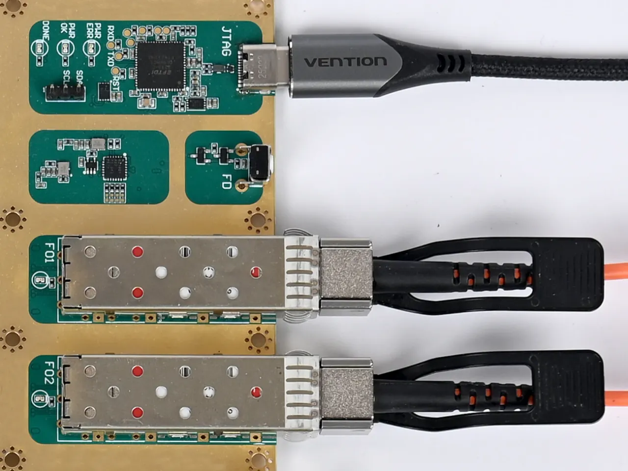
FO1 and FO2 are two SFP+ cages for 10GBASE-SR optical modules, active optical cables or passive direct-attach copper cables. Jumbo frames up to 9000 bytes are supported.
The four receive channels at 125 MS/s with 16-bit I/Q samples produce 2 × 8 Gb/s, so each link carries the data of two channels. The data is sent as UDP packets with a sequence number in every packet, so a lost or reordered packet is detected at the receiver.
The board has been tested in long transfer runs without UDP packet loss using these network cards:
- Mellanox ConnectX-5 and ConnectX-4 (10/25 GbE)
- Intel X520-DA2
- Broadcom NetXtreme II BCM57810S
- Marvell AQtion AQC100
Low latency
The receive data path from the ADCs to FO1 and FO2 is entirely FPGA logic. Samples are filtered, decimated, packed into UDP packets and sent to the network without passing through a processor or an operating system. The processor on the board only handles control and configuration.
The latency is therefore set mainly by the packet size. One packet carries 8192 bytes: 16-bit I/Q samples from two ADC channels, 1024 samples per channel. At 125 MS/s that is 8.2 µs of signal, so the host receives a packet within microseconds of the last sample in it. The sample rate and decimation are configurable, with I/Q data up to 250 MS/s; at higher rates a packet fills faster and the delay is shorter still. There is no operating system on the board to add variable delay, and the delay stays the same from one packet to the next. This matters in low-latency communication and in any system that closes a loop through the host.
GPIO and GPIO PWR
The two high-density connectors on the left and right edges of the board bring FPGA digital I/O lines out to user hardware. GPIO carries signal lines; GPIO PWR also supplies power, so a small extension board can be connected without its own supply. Typical uses are control of external RF front ends, attenuators and switches, antenna switching for direction finding, or custom interfaces implemented in the FPGA.
JTAG
The JTAG USB-C connector provides, over one cable:
- JTAG for the FPGA,
- programming of the configuration flash,
- a serial console of the Linux system running on the board.
The status LEDs next to it show the state of the power supplies (PWR OK, PWR ERR) and FPGA configuration (DONE).
FD
FD is the factory-default button. It returns the board to its default configuration, for example after a network setting has made it unreachable.
DEBUG
The 2×7 boxed DEBUG header gives service access to the board during development and production testing. It is not used in normal operation.
FAN
The 4-pin FAN header powers the cooling fan. The board dissipates about 19 W, most of it in the FPGA and the converters, and should run with forced airflow.
INPUT POWER
The board is powered from a single 10 V to 14 V DC supply through the green terminal block. The absolute maximum is 15 V. Typical consumption is 19 W with both SFP+ modules and the fan; a 12 V, 2.5 A supply is sufficient. The POWER LED next to the connector shows that input voltage is present.
Written by
Jiri Skapa · Lead RF/FPGA engineer at JSE
Jiri has designed RF and signal-processing hardware and FPGA firmware since 2003, starting with receivers and signal-processing boards for radar systems. He holds a master's degree in radio engineering from the Czech Technical University in Prague.